Finally, I have found some time to write about my final year project work. It was fun, challenging, sometimes frustrating, but most of all it was a great learning experience.
I will start with a bit of a background. My lab (RCAI.pk) is working with DFKI on a Smart Irrigation project. We have designed several iterations of prototypes for this project and others mostly based on Atmel atmega based custom built arduino boards. Atmega328 has many advantages for prototyping (Arduino Firmware and libraries… yay!) but is not “serious” enough for deployment in remote sites. Plus it is a fairly basic chip which leaves a lot to be desired. There is no on-board wireless connectivity (no, Shields don’t count), it consumes too much power to be suitable for a low-power IoT solution, has limited IO pins, and not-so-impressive peripherals.
Keeping all that in mind, and the needs of the project and lab my supervisor asked me to find a better platform which could be used as a testbed for lab’s IoT related project. Thus this project was born.
We had 3 goals:
- A mature hardware platform which can handle some serious processing, with enough IO and ADC channels to connect a 5-6 sensors simultaneously.
- Use very low power. Idea was to operate the device on a 3.3V coin cell for many months so we can do away with power harvesting
- Platform should have impressive wireless capabilities. Bluetooth Smart (or BLE) was a must.
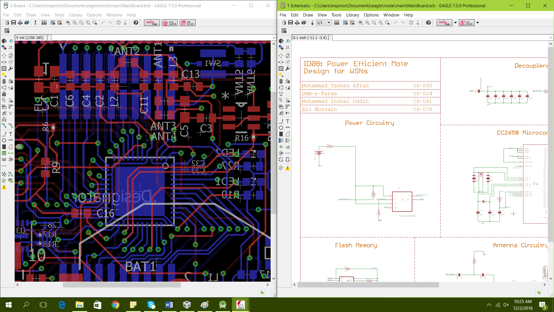
…and so we worked, and here is the proof: (Screenshot or it didn’t happen)
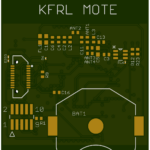
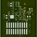
…and here are some pretty pictures generated by the PCB CAD tool.
We also made an explanatory video and an uber-mandatory project poster (don’t forget to zoom-in, it’s a high-res image.
Be First to Comment